β-Ga2O3: A new star in the power electronics field
β-Ga2O3 Power Devices
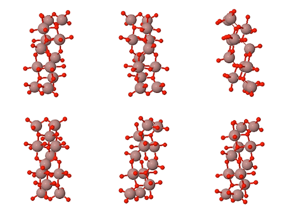
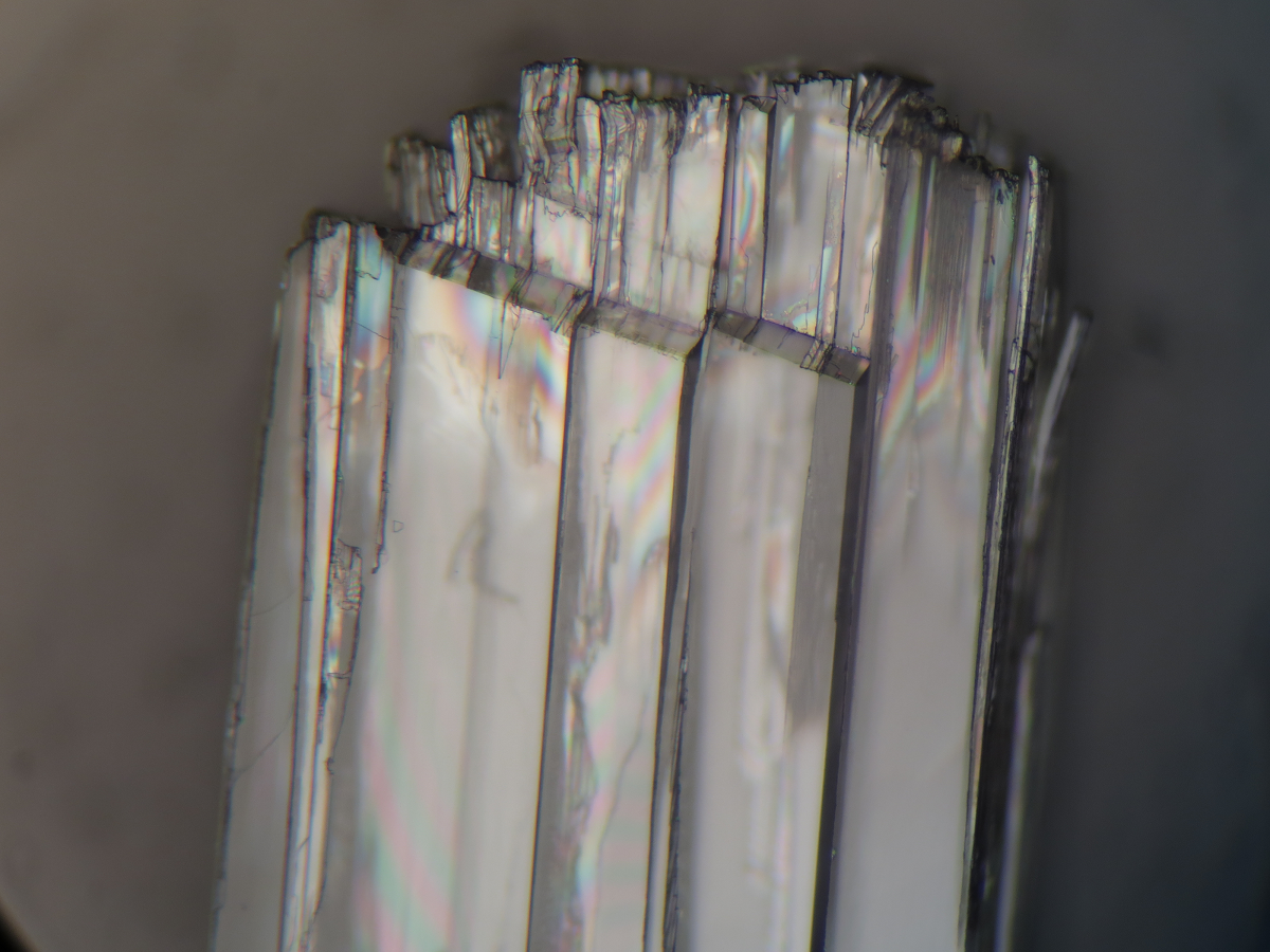
Gallium Oxide (Ga2O3), particularly its most stable form, β-Ga2O3, is a fascinating transparent oxide semiconductor with unique properties. Its exceptional wide bandgap of 4.8 eV transcends the category of “wide bandgap (WBG)” materials, placing it firmly in the realm of “Ultra-WBG” semiconductors. This opens exciting possibilities for its application in power electronics.
Doping β-Ga2O3 with Si, Ge, or Sn effectively enables n-type conductivity with remarkable efficiency. This paves the way for its potential application in the power electronics field, currently led by Silicon Carbide (SiC) and Gallium Nitride (GaN). In fact, according to Baliga's Figure of Merit (BFoM), a key measure of performance, β-Ga2O3 boasts one of the highest values among all known WBG materials. This remarkable combination of properties makes β-Ga2O3 a promising contender in the power electronics arena. Its potential to surpass established players like SiC and GaN is generating significant research interest, suggesting a bright future for this innovative material.
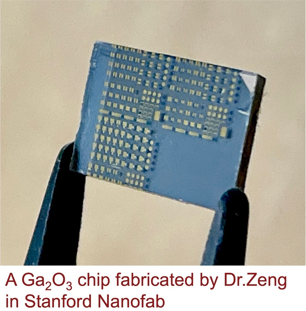
High current breakdown MOSFETs and diodes are demonstrated in Ga2O3, showing its immense potential for high power applications. RF devices are also being investigated with the hope of achieving high frequency applications. Our work is mainly on fabrication and characterization of high breakdown voltage β-Ga2O3 MOSFET. We held a few records, including the first demonstration of Ga2O3 enhancement mode MOSFET (reported in 2016 Device Research Conference), the first kilo-volt breakdown field-plated Ga2O3 MOSFET at 1.85 kV (published on IEEE-Electron Device Letters(EDL)) and the highest breakdown voltage of 8 kV among all lateral MOSFETs ever made in any material (published on IEEE-EDL, reported on various news outlets). And we are continuing working on pushing the performance boundary by using innovative power MOSFET architecutre and designs.
Engineering P-type Current Blocking Layer in β-Ga2O3
For years, achieving p-type doping in gallium oxide (Ga2O3) has remained a tantalizing challenge, a persistent thorn in the side of researchers everywhere. While Ga2O3 boasts many remarkable properties, the absence of a suitable conducting blocking layer (CBL) stands as the main obstacle to realizing its full potential in vertical devices, a crucial step for its widespread adoption.
Despite theoretical predictions suggesting inherent limitations due to self-trapping holes in the valence band, the pursuit of an effective p-type dopant has never faltered. Recent glimmers of hope have emerged with findings that magnesium and nitrogen can partially compensate electrons, illuminating a path through the previously uncharted territory. This is just the beginning of a thrilling journey: the quest for effective p-type doping or current blocking in Ga2O3 for vertical power devices. To this end, we are heavily invested in the diffusion doping technology, especially utilizing Mg doped spin-on-glass as the diffusion source, to form an effective CBL. Its success promises to propel this versatile material towards a bright future in next-generation power electronics. This era is what the experts called 'The dawn of gallium oxide microelectronics’.
Application in Power Converters
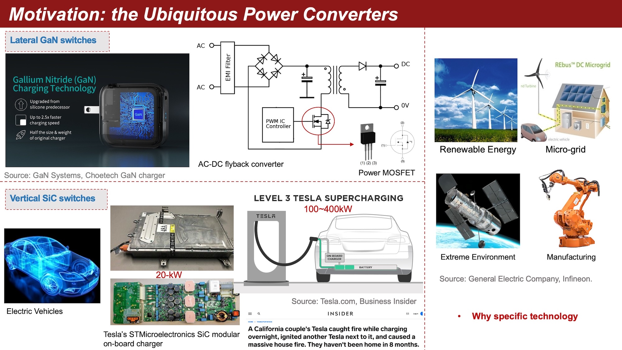
To power the growing trend of electrification across industries, from electric vehicles to renewable energy farms, we need efficient and compact technology for converting electricity. This is where wide bandgap materials like silicon carbide (SiC), gallium nitride (GaN), and gallium oxide (Ga2O3) come in. Compared to traditional silicon (Si), these materials have a much higher “bandgap” energy, allowing them to handle significantly higher power levels. By incorporating them into power conversion devices, we can dramatically reduce energy losses while also shrinking the overall size of the systems. This paves the way for advancements in electrification throughout our lives.
Superior Material Properties
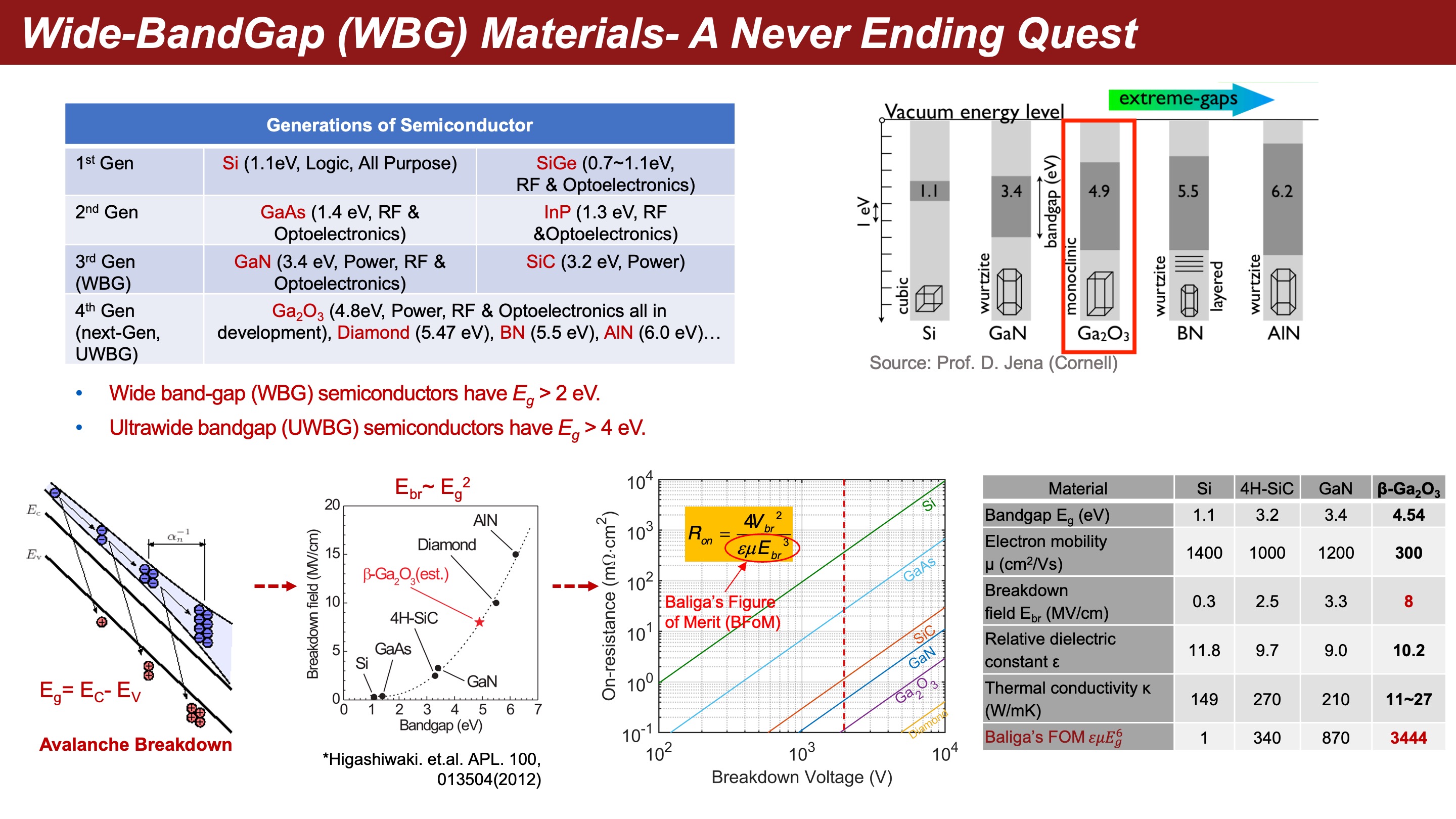
Modified Baliga's FoM
Special considerations for WBG materials
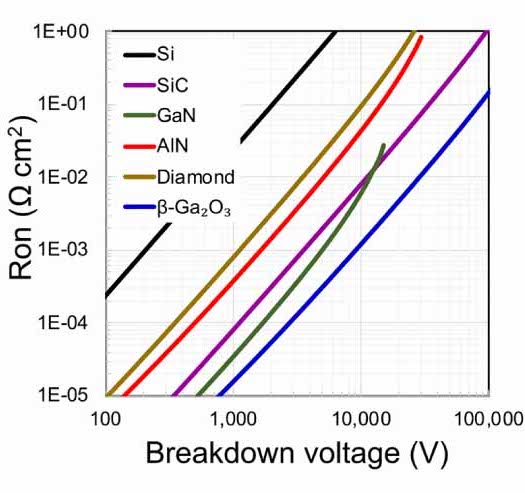
Ron-Vbr dependence considering both incomplete ionization and background compensation effects.
Ga2O3 might be THE material of choice for high power semiconductors! (*image source: Y.Zhang, J.Speck, “Semiconductor Science and Technology”, 35 125018.)
Substrate Economics
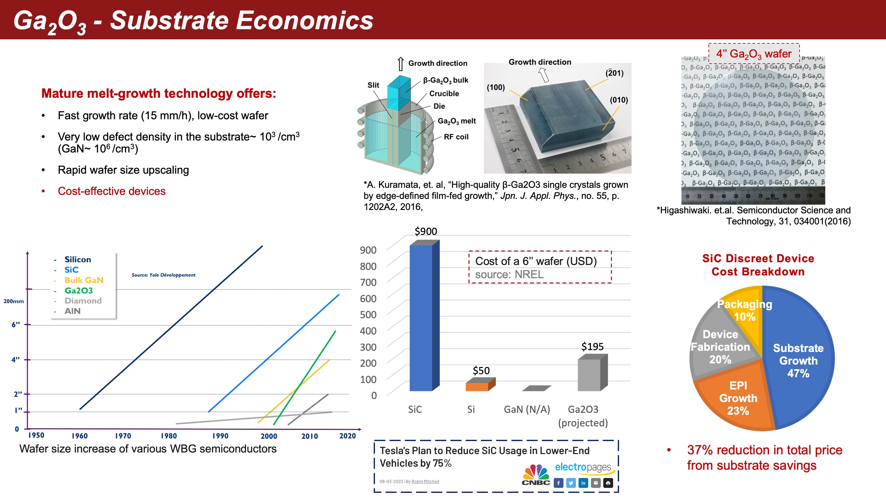
Imagine Ga2O3 power devices as affordable as silicon, thanks to well-established melt-growth technology. This method slashes costs by dramatically reducing the need for expensive substrates and epitaxial layers, which currently account for 70% of the total cost in SiC and GaN devices. This innovative technique enables Ga2O3 wafer size to grow at a rate three times faster than GaN and SiC. Remarkably, it took less than a decade to go from the first 2-inch wafer to demonstrating a 6-inch wafer, showcasing the rapid development potential.