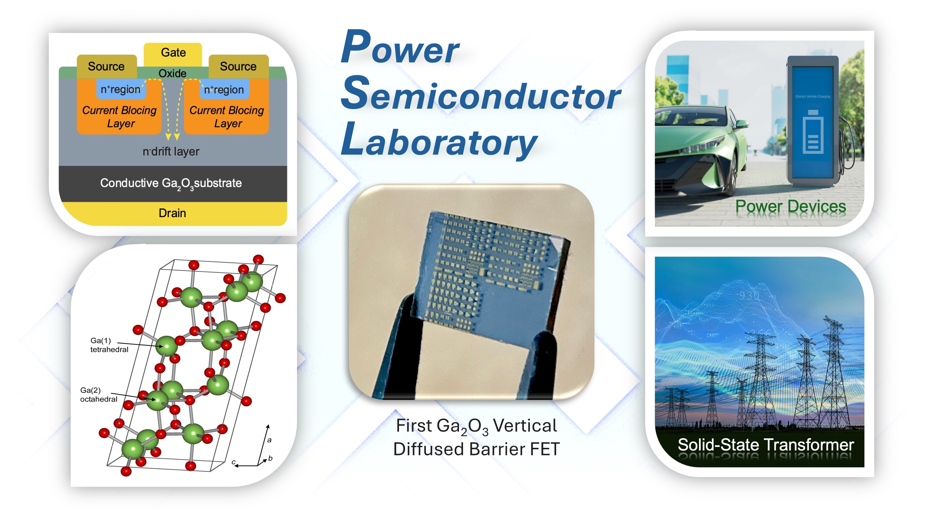
Welcome to Power Semiconductor Lab @ UNCC website. We are a group of aspiring semiconductor device engineers, aiming to crack the code of fabricating high performance vertical gallium oxide power devices.
News
Research positions are available at all levels, feel free to send an email if you are interested in joining the group.
(May, 2025) Dr. Ke Zeng published a perspective paper on Journal of Physics: Materials- “Perspective on vertical Ga2O3 power MOSFETs utilizing current blocking layer technology”.
(May, 2024) Dr. Ke Zeng is visiting Stanford University's WBG-Lab in EE Department as a visiting Professor during Summer of 2024.
(May, 2024) Dr. Ke Zeng gave an invited talk at the 245th ECS (The Electrochemical Society) meeting held at San Francisco, titled “(Invited) Breakdown Improvement of Mg-Diffused Current Blocking Layer in Ga2O3”. He also served as the chair for session “H01 - Wide-Bandgap Semiconductor Materials and Devices - Gallium Oxide 1”. More details can be found at: https://ecs.confex.com/ecs/245/meetingapp.cgi/Symposium/4786
(May, 2024) Dr. Ke Zeng published an invited paper on Applied Physics Letters, which was also selected as an editor's pick - “Simultaneous drive-in of Mg and disassociation of Mg-H complex in Ga2O3 by oxygen annealing achieving remarkable current blocking”.

“Leveraging defect to enhance doping in Ga2O3: While most efforts in semiconductor research focus on minimizing and controlling defects, we find, surprisingly, that gallium vacancy, a common defect in Ga2O3, created by high-temperature oxygen annealing, may be responsible for a dramatic increase of Mg doping density in Ga2O3 through diffusion process. This resulted in a remarkably higher breakdown voltage in the Mg-doped current blocking layer in Ga2O3, opening up new avenues for the realization of various high-power vertical Ga2O3 electron devices. Most importantly, we're seeing the promising trend where a higher Mg diffused doping unambiguously resulted in a higher vertical blocking voltage.”